Solid-state radiation detectors use crystalline semiconductors, such as silicon or germanium, to directly convert X-ray photons into electrical current. Such devices outperform other detection technologies in terms of both sensitivity and detection limit. Now, a US research team has demonstrated that a new type of solid-state X-ray detector, based on a thin film of the mineral perovskite, is 100 times more sensitive than a conventional silicon-based device (Sci. Adv. 10.1126/sciadv.aay0815).
“Our materials, hybrid perovskites, contain heavy elements such as lead and iodine that can stop X-rays more effectively than silicon,” explains corresponding author Wanyi Nie from Los Alamos National Laboratory. “In this study, we hoped to demonstrate a much thinner layer of perovskite semiconductor than silicon that can still maintain detection performance.”
The thin-film perovskite detectors could enable medical and dental imaging at extremely low radiation dose, while also boosting resolution in security scanners and X-ray research applications. “The improved lower limit of detection will allow the same quality image to be generated using a much reduced X-ray dose, which is safer for patient,” says Nie.
Device testing
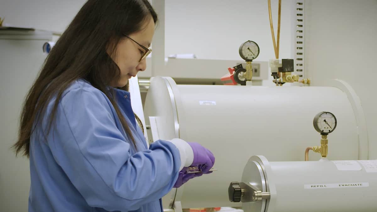
Nie and colleagues fabricated their X-ray detectors from 2D Ruddlesden-Popper (2D-RP) phase layered perovskites. They characterized the devices using a synchrotron beamline at the Argonne National Laboratory’s Advanced Photon Source.
To evaluate the feasibility of using thin-film perovskites as radiation detectors, they first determined the linear X-ray absorption coefficient as a function of incident energy for the 2D-RP perovskites, as well as for a 3D perovskite and silicon. The absorption coefficients of the perovskite materials were on average 10 to 40 times higher than that of silicon for higher-energy X-rays, with similar values seen for the 2D and 3D perovskites.
Based on the perovskites’ strong X-ray absorption, the researchers next assessed the current density–voltage characteristics of a thin-film p–i–n detector (with the structure: indium tin oxide/p-type contact/2D-RP thin film/n-type contact/gold) fabricated using a 470-nm 2D-RP thin film. As a reference, they also tested a commercial silicon p–i–n diode (600 µm thick) under the same conditions.
An important requirement for a high-performance X-ray detector is a minimal dark current at reverse bias, so that signals generated at low X-ray doses can be resolved above the dark noise. Prior to X-ray exposure, the dark current density for the 2D-RP device was 10−9 A/cm2 at zero bias. At a reverse-bias of −1 V, the dark current density was 10−7 A/cm2 – which translates to a high diode dark resistivity of 1012 W·cm.
Upon exposure to a 10.91 keV X-ray beam (with a photon flux of 2.7 × 10¹² counts/cm2/s), the 2D-RP device showed a large increase in current density at zero bias: four orders of magnitude higher than the dark current. In comparison, the current density of the silicon device only increased by two orders of magnitude.
The researchers next quantified the detection limit of the devices, by examining the X-ray-generated charge density as a function of dose under zero bias. The detecting photon density limit for the 2D-RP device was about 5×10⁸ counts/s/cm2, while the silicon device had a limit of 3×10⁹ counts/s/cm2. They attribute the superior performance of the 2D-RP device to its low dark current.
The estimated X-ray detection sensitivity of the 2D-RP device was 0.276 C/Gyair/cm3, compared with 0.000333 C/Gyair/cm3 for the silicon diode. The researchers note that the sensitivity of the 2D-RP device is considerably higher than values reported for other perovskite thin-film X-ray detectors.
One big advantage of the 2D-RP device is the high sensitivity that it exhibits under zero bias (the primary current), which enables it to operate as a self-powered detector without an external power source. This is in contrast to larger bulk perovskite detectors, which require high-voltage operation that drastically reduces the operational lifetime. Tests on the 2D-RP device revealed that the thin film is stable under both bias and X-ray exposure.
The team conclude that the layered perovskite thin film is a promising candidate for a new generation of X-ray detectors. Nie says that it should be possible to fabricate large-scale detector arrays for medical imaging applications.
“Currently, semiconductor detectors are not widely used in large-scale applications because of the cost,” she tells Physics World. “As we can fabricate our device from solution, one could imagine printing a large, pixelated detector array, which could be drastically cheaper, especially for large-scale imaging applications.”